COXEM Co., Ltd.
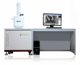
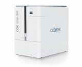
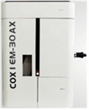
COXEM is a professional manufacturer and provider of superb solutions in Scanning Electron Microscope (SEM) and Energy Dispersive X-ray Spectroscope (EDS) for scientific and industrial purposes. COXEM also offers a specific system for your needs with an extensive know-how in nano-metrology. COXEM is a spin-off company from KRISS (Korea Research Institute of Standards Institute of Standards and Science) and our major shareholders are the governmental funds. Partner for Nano Technology Window for Nano World COXEM is a provider of superb solutions in scanning electron microscope (SEM), scanning probe microscope (SPM), confocal microscope and X-ray fluorescence spectroscope (XRF) for scientific and industrial purposes. COXEM offer a specific system for your needs with an extensive know-how in nano-metrology. We are a spin-off company from KRISS (Korea Research Institute of Standards Institute of Standards and Science) and our major shareholders are the governmental funds.Scanning Electron Microscope Versatile Tool to Access the Nano-WorldThe electron microscope is the most commonly used tool in surface metrology generally and it is widely used in educational programs, R&D and quality control. The CX-100S SEM is a powerful tool for surface characterization which produces high quality images with nano-scale resolution. The CX-100S is a classical Analytical SEM with a tungsten filament as the electron source. It offers the digital images with high resolution and image contrast by a secondary electron detector. We also supply EDS(ThermoTM) and BSE (RobinsionTM) detectors with CX-100S.Scanning Probe Microscope Evolution of Atomic Force MicroscopeSPM covers the full range scanning probe microscopy techniques to investigate the surface properties like as topography, electronic, magnetic characteristics from nano- scale to several tens of micron. The state- of-the-art DSP-based fast digital controller provides not only much easy and flexible operational interface but also sufficient high speed/resolution imaging solution. Also, our system provides very versatile Ethernet- based remote control of the SPM instrument. Advance nanolithography tool supports the very convenient interface as well as various probe-based writing techniques.Confocal Laser Scanning MicroscopeConfocal Laser Scanning Microscopy is a optical 3-dimensional surface profiler with a high-resolution. With a high numerical aperture objective lens (up to 0.95) and a shorter wavelength laser provide a high-resolution imaging along both the optical and transverse direction. A confocal pinhole also improves the imaging quality by rejecting the noise outside the focal point. Real time imaging is achieved by a fast scanning module and a signal processing algorithm. It takes less than 1 second to get the 3D surface profile of the sample. CLSM is a non-destructive high-resolution optical 3D surface profiler for the micro-structure. It is an ideal solution to measure and inspect the semiconductor wafers, FPD products, MEMS devices, glass surfaces, and material surfaces.X-Ray Fluorescence SpectroscopeXRF(X-ray Fluorescence Spectroscope) is the emission of characteristic "Secondary" (or fluorescent) X-rays from a material that has been excited by bombarding with high-energy X-rays or gamma rays. The phenomenon is widely used for elemental analysis and chemical analysis, particularly in the investigation of metals, glass, ceramics and building materials. When materials are exposed to short-wavelenght x-rays or to gamma rays, Ionisation of their component atoms may take place. Each element has electronic orbitals of characteristic energy, This Energy information shows elemental Z and the intensity of each characteristic radiation is directly related to the concentration of element in the material.